A Chemical Vapor Deposition (CVD) furnace is a critical piece of equipment used in various industries, including semiconductor manufacturing, materials science, and nanotechnology. It's designed to facilitate the deposition of thin films onto substrates through chemical reactions at high temperatures. This process is essential for creating layers with specific properties, such as semiconductors, insulators, or conductive materials, which are integral components in electronic devices.
Key Features of a CVD Furnace
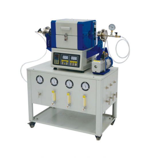
1. Temperature Control
- High-temperature uniformity across the chamber to ensure consistent deposition rates and film quality.
- Precise temperature control that can be adjusted based on the specific requirements of the material being deposited.
2. Gas Delivery System
- A sophisticated system for delivering precursor gases to the reaction chamber where they decompose or react to form the desired thin film.
- Ability to handle multiple gases simultaneously, allowing for complex layer compositions.
3. Vacuum System
- Maintains a low-pressure environment within the furnace, crucial for controlling the chemical reactions involved in the deposition process.
- Different levels of vacuum can be achieved depending on the specific requirements of the process.
4. Chamber Design
- Made from materials capable of withstanding high temperatures and reactive gases without degrading.
- Configurations that allow for easy loading and unloading of substrates, as well as quick cleaning and maintenance.
5. Automation and Control
- Advanced control systems that automate the entire deposition process, including gas flow rates, pressure, and temperature.
- Software that enables precise programming of recipes for different materials and processes, ensuring repeatability and consistency.
6. Safety Features
- Integrated safety protocols to protect operators and equipment from hazardous gases and high temperatures.
- Emergency shut-off systems and alarms to prevent accidents during operation.
Applications
- Semiconductor Industry: Used for depositing silicon dioxide, silicon nitride, polysilicon, and other materials that form the building blocks of integrated circuits.
- Solar Cell Manufacturing: Facilitates the production of thin-film solar cells by depositing layers of photovoltaic materials like cadmium telluride or copper indium gallium selenide.
- Optoelectronics: Enables the growth of compound semiconductors such as gallium arsenide and indium phosphide for use in LEDs, lasers, and photodetectors.
- Nanotechnology: Supports the synthesis of carbon nanotubes, graphene, and other nanostructured materials with unique electrical, mechanical, and thermal properties.
Quartz Tube CVD Furnace
Types of CVD Processes
- Atmospheric Pressure CVD (APCVD): Operates at standard atmospheric pressure, suitable for depositing thick films but may result in lower quality due to impurities.
- Low Pressure CVD (LPCVD): Conducted under reduced pressure to improve film uniformity and purity.
- Plasma-Enhanced CVD (PECVD): Utilizes plasma to enhance the decomposition of precursor gases, allowing for lower temperature processing and improved step coverage.
- Metalorganic CVD (MOCVD): Specifically used for growing compound semiconductors by using metalorganic compounds as precursors.
By providing precise control over the deposition process, CVD furnaces enable the creation of high-quality thin films with tailored properties, making them indispensable tools in the development and manufacture of advanced electronic devices and materials.